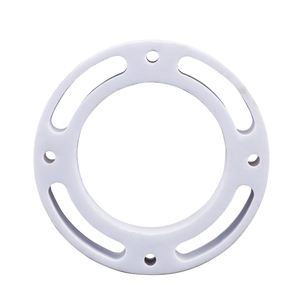
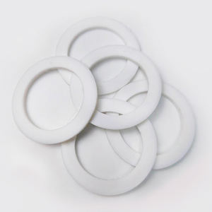
1. Material Basics and Architectural Attributes of Alumina Ceramics
1.1 Crystallographic and Compositional Basis of α-Alumina
(Alumina Ceramic Substrates)
Alumina ceramic substratums, largely made up of aluminum oxide (Al ₂ O SIX), act as the foundation of contemporary electronic product packaging due to their exceptional equilibrium of electric insulation, thermal stability, mechanical toughness, and manufacturability.
The most thermodynamically secure stage of alumina at high temperatures is diamond, or α-Al ₂ O ₃, which crystallizes in a hexagonal close-packed oxygen latticework with light weight aluminum ions inhabiting two-thirds of the octahedral interstitial sites.
This thick atomic setup conveys high hardness (Mohs 9), excellent wear resistance, and solid chemical inertness, making α-alumina suitable for harsh operating environments.
Commercial substratums usually have 90– 99.8% Al ₂ O TWO, with small additions of silica (SiO ₂), magnesia (MgO), or rare planet oxides utilized as sintering help to promote densification and control grain growth throughout high-temperature processing.
Greater pureness grades (e.g., 99.5% and over) show remarkable electrical resistivity and thermal conductivity, while lower pureness variants (90– 96%) supply cost-effective solutions for less demanding applications.
1.2 Microstructure and Flaw Design for Electronic Reliability
The efficiency of alumina substratums in digital systems is critically based on microstructural harmony and issue reduction.
A fine, equiaxed grain structure– generally varying from 1 to 10 micrometers– guarantees mechanical integrity and decreases the likelihood of fracture breeding under thermal or mechanical stress.
Porosity, especially interconnected or surface-connected pores, need to be minimized as it deteriorates both mechanical toughness and dielectric performance.
Advanced handling strategies such as tape casting, isostatic pressing, and regulated sintering in air or controlled ambiences allow the production of substratums with near-theoretical thickness (> 99.5%) and surface roughness listed below 0.5 µm, necessary for thin-film metallization and cord bonding.
In addition, impurity partition at grain limits can lead to leak currents or electrochemical migration under prejudice, necessitating strict control over raw material purity and sintering conditions to make sure lasting integrity in damp or high-voltage settings.
2. Production Processes and Substrate Manufacture Technologies
( Alumina Ceramic Substrates)
2.1 Tape Casting and Environment-friendly Body Processing
The production of alumina ceramic substrates starts with the preparation of a very dispersed slurry including submicron Al ₂ O two powder, natural binders, plasticizers, dispersants, and solvents.
This slurry is refined via tape spreading– a continuous approach where the suspension is topped a relocating carrier movie using a precision medical professional blade to accomplish consistent thickness, typically in between 0.1 mm and 1.0 mm.
After solvent evaporation, the resulting “green tape” is adaptable and can be punched, drilled, or laser-cut to create by means of openings for upright affiliations.
Several layers might be laminated to develop multilayer substratums for complicated circuit combination, although most of commercial applications use single-layer configurations because of cost and thermal development considerations.
The green tapes are after that meticulously debound to remove natural additives via managed thermal decay before final sintering.
2.2 Sintering and Metallization for Circuit Assimilation
Sintering is conducted in air at temperature levels in between 1550 ° C and 1650 ° C, where solid-state diffusion drives pore elimination and grain coarsening to accomplish complete densification.
The direct contraction during sintering– commonly 15– 20%– must be specifically anticipated and compensated for in the design of environment-friendly tapes to ensure dimensional accuracy of the last substratum.
Complying with sintering, metallization is put on form conductive traces, pads, and vias.
2 primary techniques control: thick-film printing and thin-film deposition.
In thick-film modern technology, pastes containing metal powders (e.g., tungsten, molybdenum, or silver-palladium alloys) are screen-printed onto the substratum and co-fired in a minimizing ambience to form durable, high-adhesion conductors.
For high-density or high-frequency applications, thin-film procedures such as sputtering or evaporation are used to deposit attachment layers (e.g., titanium or chromium) complied with by copper or gold, making it possible for sub-micron patterning through photolithography.
Vias are full of conductive pastes and terminated to establish electric affiliations in between layers in multilayer designs.
3. Practical Properties and Performance Metrics in Electronic Solution
3.1 Thermal and Electric Habits Under Operational Tension
Alumina substratums are prized for their positive mix of moderate thermal conductivity (20– 35 W/m · K for 96– 99.8% Al Two O SIX), which makes it possible for effective heat dissipation from power tools, and high volume resistivity (> 10 ¹⁴ Ω · cm), making sure very little leakage current.
Their dielectric consistent (εᵣ ≈ 9– 10 at 1 MHz) is steady over a large temperature level and frequency variety, making them appropriate for high-frequency circuits as much as numerous gigahertz, although lower-κ materials like aluminum nitride are favored for mm-wave applications.
The coefficient of thermal development (CTE) of alumina (~ 6.8– 7.2 ppm/K) is reasonably well-matched to that of silicon (~ 3 ppm/K) and specific packaging alloys, decreasing thermo-mechanical stress during device operation and thermal biking.
However, the CTE inequality with silicon remains a problem in flip-chip and direct die-attach setups, commonly needing compliant interposers or underfill materials to alleviate fatigue failure.
3.2 Mechanical Effectiveness and Environmental Sturdiness
Mechanically, alumina substratums display high flexural toughness (300– 400 MPa) and excellent dimensional stability under lots, enabling their usage in ruggedized electronic devices for aerospace, vehicle, and industrial control systems.
They are resistant to resonance, shock, and creep at raised temperatures, keeping architectural stability up to 1500 ° C in inert ambiences.
In damp environments, high-purity alumina shows very little moisture absorption and outstanding resistance to ion migration, guaranteeing long-term dependability in exterior and high-humidity applications.
Surface solidity also safeguards versus mechanical damages throughout handling and setting up, although care needs to be required to prevent side chipping because of inherent brittleness.
4. Industrial Applications and Technical Impact Throughout Sectors
4.1 Power Electronics, RF Modules, and Automotive Systems
Alumina ceramic substratums are common in power electronic modules, consisting of shielded gate bipolar transistors (IGBTs), MOSFETs, and rectifiers, where they supply electric isolation while facilitating warmth transfer to warm sinks.
In radio frequency (RF) and microwave circuits, they serve as service provider platforms for hybrid incorporated circuits (HICs), surface area acoustic wave (SAW) filters, and antenna feed networks due to their secure dielectric residential properties and low loss tangent.
In the vehicle sector, alumina substrates are utilized in engine control devices (ECUs), sensing unit bundles, and electric lorry (EV) power converters, where they endure heats, thermal cycling, and exposure to corrosive fluids.
Their integrity under rough problems makes them crucial for safety-critical systems such as anti-lock braking (ABS) and progressed driver support systems (ADAS).
4.2 Clinical Instruments, Aerospace, and Arising Micro-Electro-Mechanical Solutions
Past consumer and industrial electronic devices, alumina substratums are used in implantable medical gadgets such as pacemakers and neurostimulators, where hermetic securing and biocompatibility are critical.
In aerospace and protection, they are utilized in avionics, radar systems, and satellite interaction modules as a result of their radiation resistance and security in vacuum cleaner atmospheres.
In addition, alumina is significantly utilized as a structural and insulating platform in micro-electro-mechanical systems (MEMS), consisting of pressure sensors, accelerometers, and microfluidic devices, where its chemical inertness and compatibility with thin-film handling are helpful.
As electronic systems remain to demand greater power thickness, miniaturization, and dependability under severe conditions, alumina ceramic substratums remain a foundation product, connecting the void in between performance, expense, and manufacturability in sophisticated electronic product packaging.
5. Distributor
Alumina Technology Co., Ltd focus on the research and development, production and sales of aluminum oxide powder, aluminum oxide products, aluminum oxide crucible, etc., serving the electronics, ceramics, chemical and other industries. Since its establishment in 2005, the company has been committed to providing customers with the best products and services. If you are looking for high quality alumina ceramic components, please feel free to contact us. (nanotrun@yahoo.com)
Tags: Alumina Ceramic Substrates, Alumina Ceramics, alumina
All articles and pictures are from the Internet. If there are any copyright issues, please contact us in time to delete.
Inquiry us